
An array of 11 metasurface-based optical spectrometers, pictured here before the final fabrication step. Image credit: Faraon Lab/Caltech
Throughout history, the optical system has a major application and also been a key technique and component in the wide ranges of science and technology. As we became more and more advance, we are also required to have more and more advanced tools. As the application of optical spectrometry is rapidly increasing, we also have a large demand for spectrometers and/or spectrum analyzers with different properties (e.g., operation bandwidth, resolution, size, etc.) required for different applications. Conventional optical spectrometers are composed of a dispersive element, such as a prism or a diffraction gating, that deflects different wavelengths of light by different angles, followed by focusing elements that focus light incoming from different angles to different points (or lines). The main components are comprised of the fore-optics section, diffraction grating, focusing lenses, and detector array.
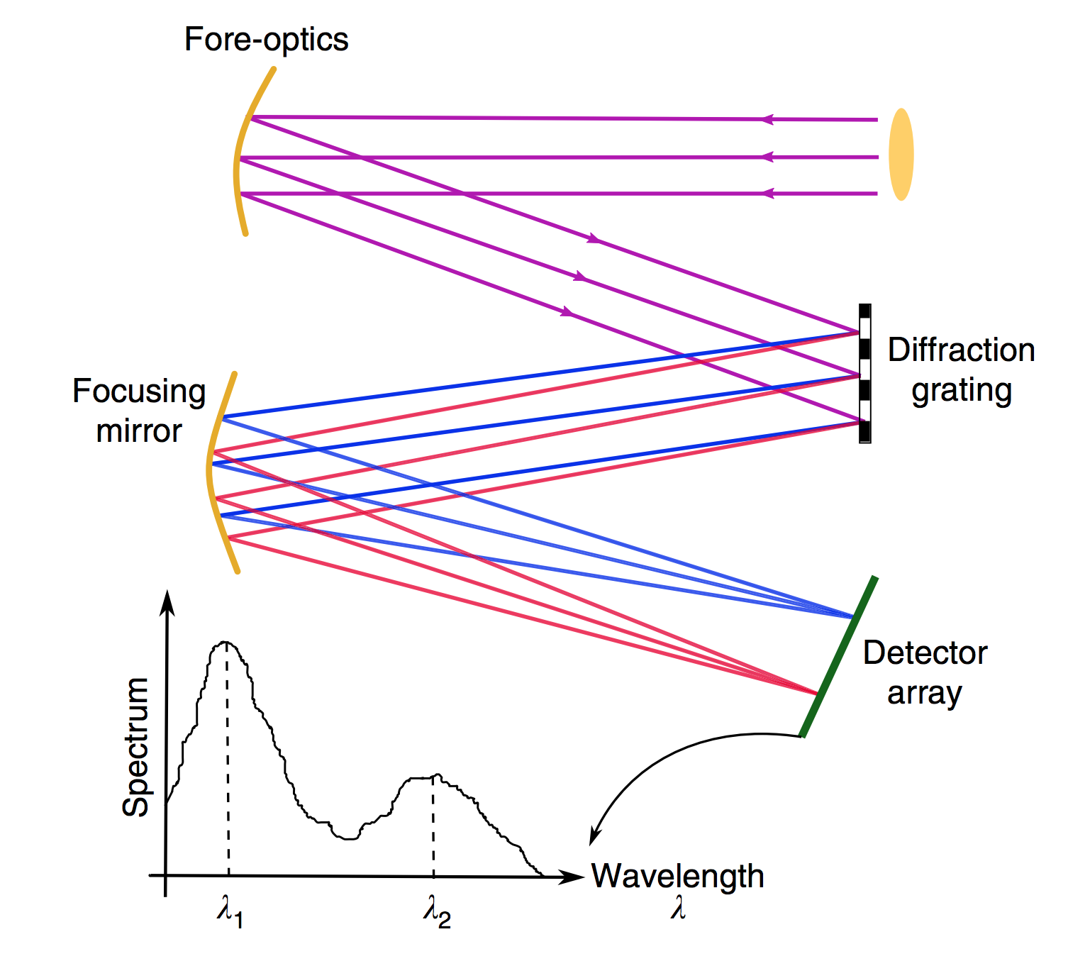
These combinations of several free-space optical elements like grating elements, focusing mirrors, etc. results in bulky spectrometers design. Various schemes and structures have been investigated for the realization of such spectrometers but none gives a compact solution.
But a team of researchers from California Institute of Technology (Caltech), have introduced the concept of folded metasurface optics. They experimentally demonstrated a compact spectrometer made from a 1-mm-thick glass slab and the designed spectrometer has a resolution of ~1.2 nm. A paper describing their work was published in the journal Nature Communication, on 10 October 2018.
The proposed scheme for a new folded compact spectrometer is shown below.
They claimed the designed folded metasystem can be applied to many optical systems, such as optical signal processors, interferometers, and computational optical systems and this will help us in significantly reducing the sizes of the spectrometer and also increase the mechanical potential for their integration.
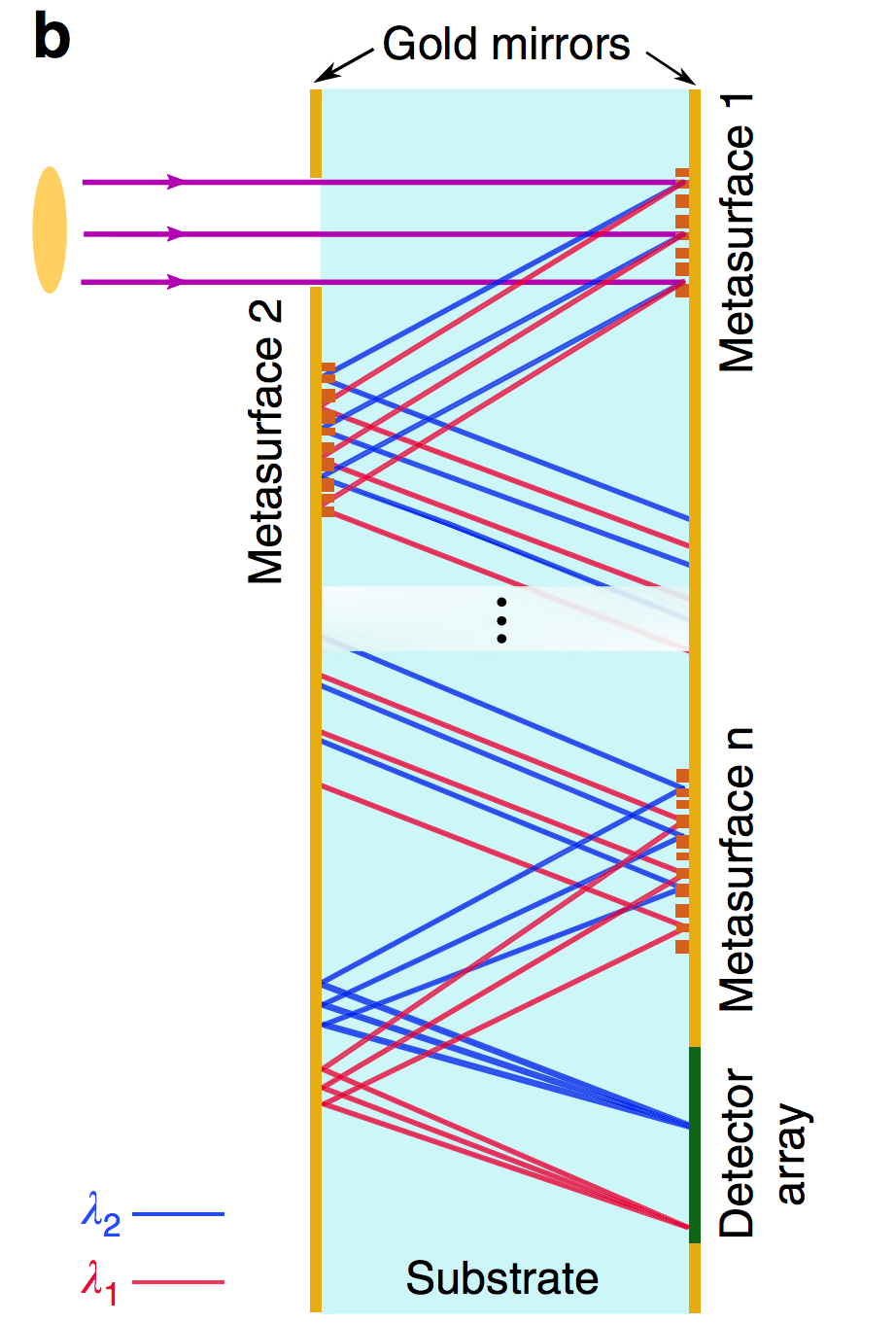
The team demonstrated a folded optical metasystems with multiple metasurfaces integrated on a single substrate. Here the main advantage was that the integrated multiple metasurfaces also play the role of propagation space for light. They claimed this achievement as the first demonstration of an optical metasystem that is comprising more than two metasurfaces.
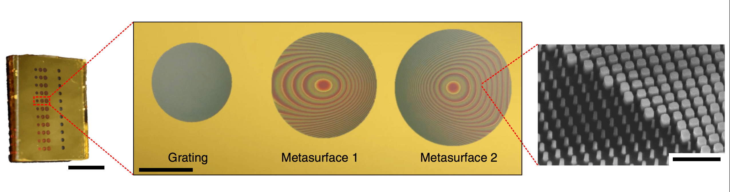
The device consisted of three metasurfaces that are all patterned on one side of a 1-mm-thick fused silica substrate. The first metasurface was a periodic blazed grating with a period of 1 μm. This grating helped them to disperse different wavelengths of the collimated input light to different angles. The second and third metasurfaces focus light coming from different angles to different points on the focal plane. The input angle corresponds to various input wavelengths.
The focal plane was designed to be located 200 μm outside the substrate. This asymmetric design will help us in integrating the spectrometer and also makes the detector array much simpler. This results in a more compact and mechanically robust device allowing us for direct integration into consumer electronic products like smartphones.
Each of the meta-atoms consisted of a rectangular α-Si nano post, capped by a 2-μm-thick SU-8 layer, and backed by a gold mirror. The post height and lattice constant were 395 and 246 nm, respectively. These values were chosen accordingly to achieve full 2π phase coverage while minimizing the variation of the reflection phase derivative across the band. By decreasing the wavelength dependence of the phase profiles, minimizing the phase derivative variation will mitigate the reduction of device efficiency over the bandwidth of interest.
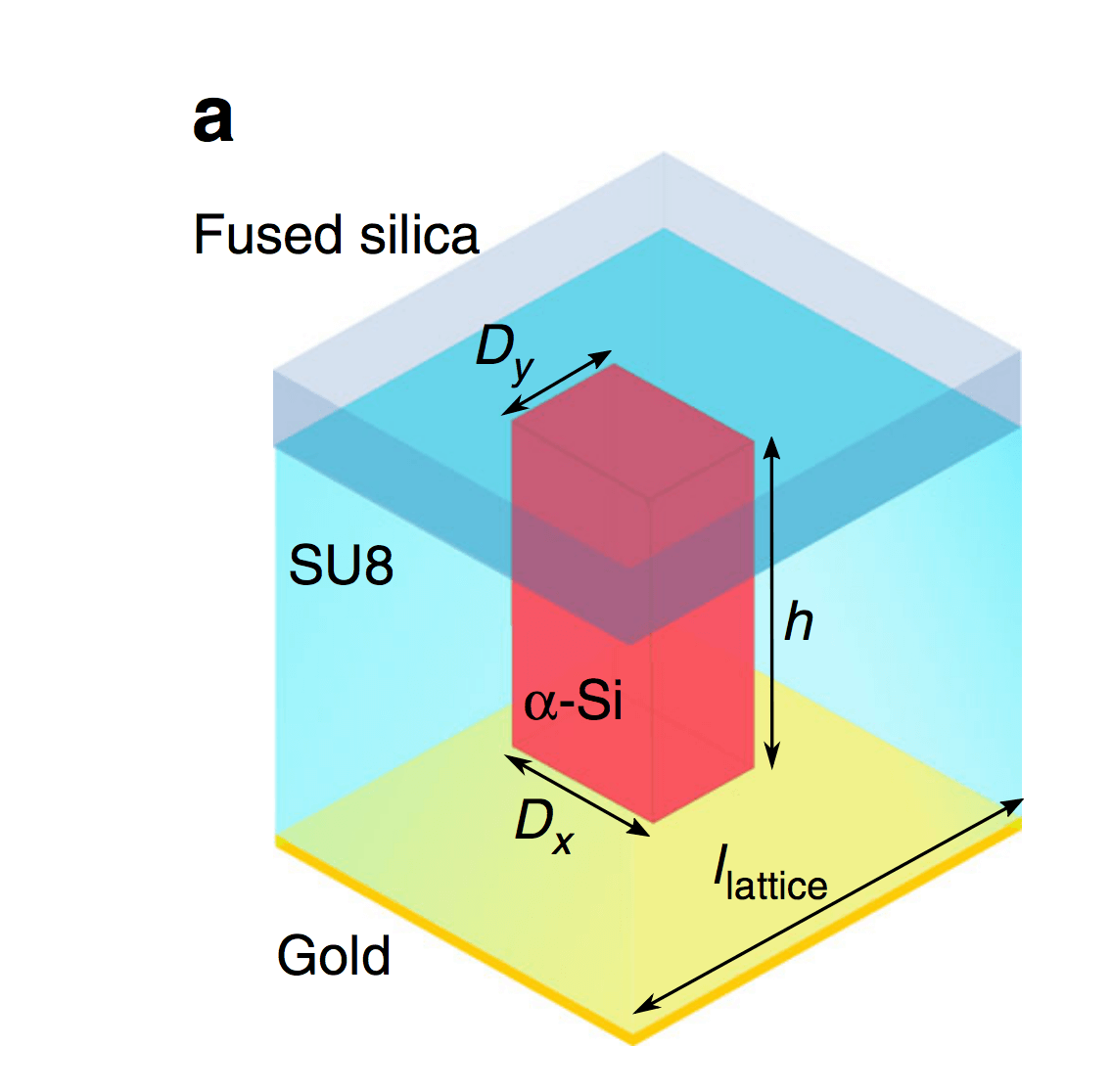
The nanopost with the rectangular cross-section helped them to minimize the difference in reflection amplitude and phase for the transverse electric and magnetic polarizations.
Now a starting point using the recently developed high-NA lens design method was selected and the structure was then optimized using the particle swarm optimization algorithm.
A periodic phase profile of the blazed grating will deflect the normally incident light to a larger-angle inside the substrate.
The team fabricated the new optical design at the Kavli Nanoscience Institute. For the fabrication they used conventional micro- and nano-fabrication technique which is shown in the figure below.
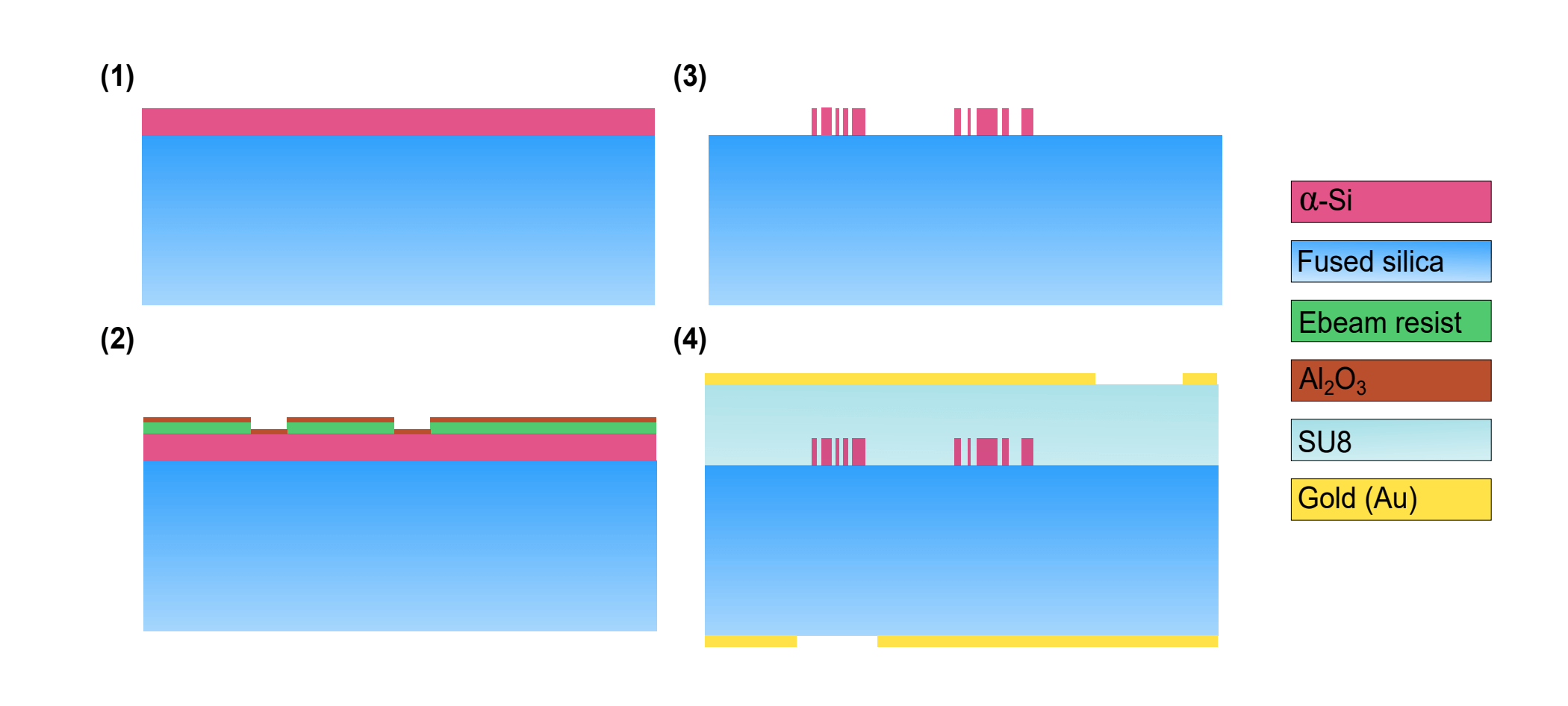
First, a 395-nm-thick layer of α-Si was deposited on a 1-mm-thick fused silica substrate using Plasma-enhanced chemical vapor deposition (PECVD) technique. All metasurfaces were then patterned using electron beam lithography and subsequently followed by a pattern inversion through the lift-off and dry etching processes.
Both sides of the patterned metasurface were covered with the SU-8 layer. The metasurfaces were capped by a ~2-μm-thick SU-8 layer. A gold layer of thickness 100-nm was deposited as the reflector agent. A second reflective gold layer was deposited on the second side of the substrate. An optical microscope image of the three metasurfaces, along with a scanning electron micrograph of a part of the fabricated device is shown.
Then to experimentally characterize the spectrometer, a normally incident collimated beam from the laser was targeted on the input aperture of the device. The beam they used was tunable and to image the focal plane, a custom-built microscope was used outside its output aperture.
Researchers successfully demonstrated a 1-mm-thick spectrometer and the spectrometer has a resolution of ~1.2 nm over a 100-nm bandwidth (>12%) in the near-infrared.
Here the measured efficiency of the spectrometer demonstrated was about 25%. The team is hopeful about using mirrors with higher reflectivity and anti-reflection coatings on the input and output apertures. this value can be significantly increased to about 70%.
In the experiment, the metasurface spectrometers were fabricated in a batch process but they can also be fabricated on the same chip. By encompassing multiple operation bandwidths and by fabricating multiple spectrometers on the same chip, the production cost of this device can be significantly reduced.
Moreover, by improving the angular response of the current device one can design a compact hyperspectral imager capable of simultaneous one-dimensional imaging and spectroscopy. Involved researchers expect that the proposed platform will also be used for on-chip interferometers, imaging systems, and other devices performing complex transformations of the field.
Reference and Further Reading:
-
Faraji-Dana, M., Arbabi, E., Arbabi, A. et al. Compact folded metasurface spectrometer. Nat Commun 9, 4196 (2018). https://doi.org/10.1038/s41467-018-06495-5